


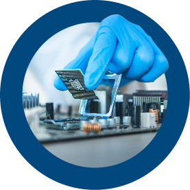
YOUR TRUSTED PARTNER IN WATER TREATMENT SOLUTIONS FOR THE ELECTRONICS & SEMICONDUCTOR INDUSTRIES
IDE’s solutions help electronic & semiconductor manufacturers manage wastewater, meet stringent water quality standards, and optimize production processes.
The manufacturing of semiconductors and electronic devices demands substantial volumes of ultrapure water (UPW) and results in significant wastewater production. At IDE Technologies, we specialize in providing water treatment solutions tailored specifically to the unique requirements of the semiconductor and electronics industries. Our cutting-edge technologies and innovative approaches meet the exceptionally stringent standards of these sectors.
IDE solutions for Semiconductor FAB process wastewater and End of Pipe (EOP) stages help Electronics and Semiconductor plants tackle their water challenges effectively – cutting costs, minimizing environmental impact, and reducing regulatory risks:
- Reuse, Reclaim & Recycle Systems
Our systems treat various streams within the wafer production process, reducing effluent waste discharge, minimizing raw water consumption, and protecting the environment. - End of Pipe (EOP) Wastewater Treatment
Managing wastewater from semiconductor manufacturing presents unique challenges due to stringent discharge requirements. Our advanced technologies optimize water management for this critical stage.
IDE’s solutions help electronic & semiconductor manufacturers manage wastewater, meet stringent water quality standards, and optimize production processes, while reducing carbon and water footprint and supporting advanced ESG policies.
IDE’s Key Offerings:
- Standard Reverse Osmosis (RO) and Filtration Systems
We provide RO and filtration systems (GAC, UF, Sand Filters) to handle diverse water streams within semiconductor manufacturing processes.
- Specialized Treatment for Complex Streams
For streams requiring specific treatment (such as CMP, ammonia waste, HFW plating, scrubber), we utilize a specialized treatment chain involving UF and PFRO technologies with clarifiers, focusing on reuse, reclaim, and recycle strategies.
- Biological Treatment with MBR (Membrane Bioreactor)
We integrate MBR technology to efficiently treat various streams, preparing them for subsequent treatment stages.
- High Recovery Reclaim Technologies
Our proprietary MaxH2O PFRO and MaxH2O Desalter systems deliver exceptional recovery rates, reduce chemical usage, enhance water reuse, lower water footprints, and facilitate efficient Zero Liquid Discharge (ZLD) implementation.
- Zero Liquid Discharge (ZLD) Solutions
Essential for regulatory compliance and sustainability, our ZLD solutions, including the MaxH2O Desalter, ensure minimal environmental impact.
Innovative Project Execution with MPD
IDE excels with its unique Off-Site Manufacturing (OSM) approach, also known as Modular Pre-assembly Design (MPD). This methodology significantly reduces project timelines, ensures high-quality outcomes, and optimizes both capital expenditures (CapEx) and operational expenditures (OpEx).
Upgrades and Enhancements
IDE offers comprehensive upgrades to existing systems, including advanced MaxH2O solutions for high recovery such as PFRO and Desalter systems. We also provide custom semiconductor wastewater treatment packages where needed.
Our PFAS Removal Solutions
The EPA has recently confirmed a new PFAS (Per- and Polyfluoroalkyl Substances) roadmap which establishes legally binding maximum contaminant levels to protect against these persistent “forever chemicals” in drinking water. The CERCLA regulation designates PFAS as hazardous substances, which enables the EPA to hold parties responsible for PFAS contamination liable for cleanup costs. This regulation also facilitates federal and state cleanup actions and requires reporting of PFAS releases over specific thresholds. Industries reliant on PFAS compounds may face more heightened scrutiny and regulatory pressures in the near future. At IDE we offer a complete range of PFAS removal solutions for treating municipal and industrial wastewater prior to discharge.
Find out more about overcoming PFAS challenges in semiconductor manufacturing
IDE delivers a full spectrum of water solutions, including:
- Feasibility and Water Studies
Analyzing water needs and identifying opportunities for optimizing existing facilities - Strategic Partnerships
Providing expert guidance before and during bidding process to support decision-making processes for new water projects - Technology Expertise
Offering engineering, procurement, and construction (EPC) services, along with operation and maintenance (O&M) solutions - Water-as-a-Service
Leveraging our technological expertise, project management skills, and strong financial partnerships to plan, finance, develop, own, and manage cutting-edge water projects
Learn more about Overcoming PFAS Challenges in Semiconductor Manufacturing
Related Solutions
All solutions


FAQ
Water is essential to nearly every stage of semiconductor manufacturing. It is used for wafer rinsing, chemical dilution, surface preparation, CMP (chemical mechanical polishing), photolithography, etching, cooling, and maintaining cleanroom humidity standards. The majority of water demand comes from producing and rinsing wafers, where even microscopic contaminants can cause defects. As fabrication processes become more advanced, water quality requirements continue to tighten, and the overall volume of water needed per wafer increases.
A modern semiconductor fab can use up to 10 million gallons of water per day, depending on production capacity and the technologies being manufactured. Advanced nodes, high-volume production, and 24/7 operation all increase water usage. Large fabs often rival the water consumption of a small city. Most of this water must be treated to ultrapure standards and reused multiple times to meet both production and sustainability requirements.
“Semiconductor facilities require different grades of water for different applications, including: Ultrapure Water (UPW): for wafer rinsing, lithography, and CMP High-purity process water: for chemical dilution and tool cleaning Cooling water: for HVAC, chillers, and process equipment Wastewater streams: from chemical drains, rinses, CMP, etching, etc. UPW is the most critical and represents the highest production cost due to the advanced treatment steps required.”
UPW is the backbone of semiconductor manufacturing. Every wafer is rinsed hundreds of times throughout the process, and even a single particle or ion can cause a defect that renders an entire chip unusable. UPW must meet extremely low limits for dissolved solids, organics, particles, bacteria, and silica. Treating water to this level requires multiple steps including reverse osmosis, ion exchange, ultrafiltration, UV oxidation, degasification, and polishing.
Water-intensive processes include:
CMP (Chemical Mechanical Polishing)
RCA cleaning sequences
Wet etching and stripping
Multiple rinse cycles in wafer cleaning
Cooling systems and scrubbers
CMP alone can represent 30–40% of a fab’s total wastewater volume.
UPW systems remove:
Dissolved ions (Na, Ca, K, Cl, SO₄)
Silica and colloidal silica
Total Organic Carbon (TOC)
Particles down to sub-10 nm
Microorganisms and endotoxins
Dissolved gases such as oxygen and carbon dioxide
UPW purity levels far exceed those required in pharmaceuticals or power generation, which is why semiconductor-grade water production is among the most stringent in the world.
UPW production involves a multi-barrier approach:
Pretreatment: softening, multimedia filtration
Reverse Osmosis: removes most ions, TOC, and dissolved solids
Electrodeionization (EDI): further reduces ionic content
UV oxidation: breaks down organic contaminants
Ultrafiltration: removes submicron particles
Degasification: removes dissolved gases
Polishing loops: ensure stable quality at point-of-use
This ensures water meets the extremely low contaminant thresholds required for leading-edge chip production.
Membrane filtration (UF, NF, RO) provides high rejection of particles, organics, and dissolved salts. In semiconductor facilities, RO is used for bulk ion removal, while UF is used to eliminate nanometer-scale particles that could interfere with photolithography or etching processes. Advanced membrane configurations enable high recovery while maintaining stringent UPW standards.
Semiconductor wastewater is complex because it contains:
Highly variable chemical compositions
HF, HCl, H₂SO₄, NH₃, and other chemical residues
Metals such as copper, nickel, and tungsten
CMP slurry particles
Solvents, organics, and photoresists
PFAS and emerging contaminants
These streams cannot be mixed unchecked and often require segregated treatment lines. pH fluctuations, abrasive solids, and microcontaminants add further complexity.
Common contaminants found in semiconductor wastewater streams include:
Fluorides from etching processes
Slurries from CMP
Metals from deposition and CMP
Solvents and organics from photoresist removal
Ammonia and nitrogen compounds
Acids and alkaline chemicals
PFAS from specialty chemistries
Each stream requires tailored pretreatment before it enters centralized recovery or discharge systems.
Treatment typically involves a combination of:
pH neutralization
Precipitation/clarification
UF/RO for dissolved contaminants
Advanced Oxidation Processes (AOPs)
Metals removal through chemical or membrane processes
High-recovery RO or thermal systems for water recycling
Modern fabs aim to maximize reuse while reducing waste volumes and environmental impact.
Key concerns include:
High fluoride levels from etching
Heavy metals
High TOC levels
PFAS contamination
Solvent residues
Nitrogen compounds
Large volumes of wastewater with variable loads
Strict global and regional regulations make monitoring and control essential.
Discharge is governed by local environmental authorities, but semiconductor-specific concerns are addressed by:
U.S. EPA industrial effluent guidelines
EU Water Framework Directive
Taiwanese EPA semiconductor discharge standards
Korean National Effluent Standards
Emerging global PFAS regulations
Many regions now mandate water recycling thresholds as part of fab permitting.
PFAS compounds are chemically stable, resistant to conventional oxidation, and difficult to remove. Effective approaches include:
High-pressure membrane filtration
Activated carbon adsorption
Ion exchange resins
Advanced oxidation combined with specialized destruction technologies
The industry is under increasing pressure to eliminate PFAS discharges completely in semiconductor wastewater.
Membrane processes include:
UF: for removing CMP solids and particulates
NF: for selective removal of multivalent ions
RO: for desalination and high-purity water recovery
MBR: for treating specific organic-rich streams
Selecting the right combination ensures efficient removal of metals, organics, and dissolved solids.
IDE use AOPs to deal with fouling in wastewater tretment. AOPs generate hydroxyl radicals — highly reactive species that break down otherwise persistent organic compounds. In semiconductor streams, AOPs are used to degrade photoresists, solvents, surfactants, and trace organics before membrane treatment. UV/H₂O₂, ozone, and advanced catalytic systems are commonly used.
The core reaction involves the formation of hydroxyl radicals (•OH) with oxidation potentials high enough to attack carbon bonds. These radicals convert organic molecules into CO₂, water, and simpler biodegradable compounds. This improves downstream RO performance and helps meet stringent discharge limits.
Water recycling captures wastewater from processes such as rinsing, CMP, and wet etching, treats it through a combination of membranes and polishing steps, and returns it to the UPW or cooling systems. Semiconductor recycling systems often include high-recovery RO, brine concentration, and continuous monitoring to ensure safety in reuse applications.
Safety is ensured through:
Segregation of incompatible streams
Multistep treatment including RO, NF, UF, and AOPs
Continuous online monitoring
Redundant polishing stages
High-purity storage and distribution
Fabs often treat water beyond regulatory requirements to protect process integrity.
State-of-the-art fabs can recover up to 85–90% of their wastewater using high-recovery RO, advanced filtration, and thermal polishing technologies. Some facilities pursuing zero liquid discharge (ZLD) can achieve even higher recovery levels.
Challenges include:
High variability in wastewater composition
Fine CMP particles and abrasive solids
High fluoride levels
Organic solvents and photoresists
PFAS contamination
Scaling and fouling risks in high-recovery systems
Advanced pretreatment and specialized RO configurations are critical.
Semiconductor fabs are major water consumers, and most are located in water-stressed regions. Recycling reduces dependence on municipal water, stabilizes supply for uninterrupted production, reduces environmental impact, and improves water sustainability metrics. Most leading fabs now treat water efficiency as a strategic advantage.
Effective water consumption strategies in semiconductor fabs include:
High-recovery RO systems
CMP wastewater polishing and reuse
Optimizing UPW production efficiency
Closed-loop cooling water systems
Segregated wastewater treatment
Advanced monitoring to prevent unnecessary rinsing
Leading fabs pair these solutions with long-term water stewardship initiatives.
Companies are investing in:
High-efficiency water recycling
Zero liquid discharge (ZLD) programs
Supply chain water offsets
Digital water monitoring
Reducing chemical usage in wet processes
Designing fabs with circular water loops from the start
Water sustainability is now central to fab design, permitting, and ESG commitments.
Strategies include water source diversification, recovery optimization, wastewater segregation, smart metering, and energy-efficient treatment technologies. Pairing membrane and thermal systems enables high recovery while minimizing operational costs and environmental footprint.
Water recycling reduces dependency on external water sources, lowers operational risk, and stabilizes long-term production. As fabs scale to meet global chip demand, water resilience becomes essential for securing permits and ensuring uninterrupted output.
Trends include:
High-recovery RO designed for complex chemistries
PFAS removal and destruction technologies
Low-temperature evaporators
Membrane distillation for brine concentration
AI-powered plant optimization
More modular, scalable water plants for new fabs
These innovations support higher throughput with lower water intensity.
Advanced analytics and AI monitor pH, flow, TOC, ions, and contaminant spikes in real time. Predictive models help prevent fouling, optimize chemical dosing, and reduce energy use, ultimately improving recovery and lowering OPEX.
Key innovations enabling higher water recovery in the semiconductor sector include:
High-shear RO for challenging streams
Slurry-resistant UF membranes
Hybrid MLD/ZLD systems
Advanced antiscalants tailored for semiconductor chemistries
Integrated wastewater segregation frameworks
These solutions help fabs approach 90%+ recovery safely and cost-effectively.
Contact an IDE Expert
Would you like more information about our technologically advanced solutions for the Microelectronics & Semiconductors industry?


